Solid State Tesla Coil
Background:
A Tesla coil is a large, air-cored resonant transformer used to demonstrate basic concepts of electromagnetism, and prized by many hobbyists for producing bursts of showy arcs from the top of the secondary coil. Whereas a typical transformer serves to transfer power from the primary to the secondary coils as efficiently as possible, resonant transformers attempt to store energy. Traditional spark gap Tesla coils (SGTCs) use a neon sign transformer (NST) to step mains voltage up to over 1 kV, charging a high-voltage capacitor in series with the output of the transformer, and in parallel with the primary output coil. NSTs are typically preferred over standard power transformers due to the placement of a current-limiting magnetic shunt into the iron core, allowing a secondary path for the magnetic flux to bypass the secondary winding and thereby limiting current output and protecting the circuit from drawing exceedingly large amounts of power. The NST in a SGTC will charge the capacitor until a sufficient electric field exists as to cause dielectric breakdown of the air in between the eponymous spark gap, which sits in series with the primary coil, and separates it from the capacitor, such that current will not flow to the primary coil while the capacitor is charging. At this point, the air will conduct current from the capacitor through the primary coil, which in turn induces a greater step up in potential at the secondary coil. A (usually toroidal) topload attached to the secondary coil forms a capacitive coupling with the ground, allowing arcs to form from the corners of the topload. This process repeats many times per second, creating a striking visual phenomenon resembling lighting.
The solid state Tesla coil (SSTC) operates on a different principle. The initial voltage supplied to an SSTC is typically much lower than for a SGTC, eliminating the need for an NST. Instead of relying on the buildup of charge in a capacitor to trigger a spark, a transistor is used as a switch to open and close the path from the primary to ground, as shown in Fig 1. An added benefit of these circuits is that they automatically tune themselves to the resonance frequency of the secondary coil, by affecting the rate at which the transistor turns on and off.
The physics of SSTCs is perhaps foremost governed by Lenz' and Faraday's Laws. Faraday's Law provides that a changing magnetic field will induce an electromotive force (EMF) in an electric circuit, while Lenz' law provides that the induced current will flow in the direction which creates a magnetic field opposing the inducing field. These Laws are typically expressed conjointly as $$\begin{align} \varepsilon = -N\frac{\Delta\phi}{\Delta t}, \end{align}$$ where $\varepsilon$ is the EMF in volts, $N$ is the number of homogeneous loops in the conductor, and $\phi$ is the magnetic flux in volt-seconds. The direction given by Lenz' law appears as the negative sign preceding the equation.
The step up in voltage of two inductors that form a transformer can be derived from this law by considering the EMF and number of turns $N$ for both coils, which share a magnetic flux between them. This can be written for primary and secondary inductors $L_p$ and $L_s$ as $$\begin{align} \varepsilon_p = -N_p\frac{\Delta\phi}{\Delta t} \nonumber\ \varepsilon_s = -N_s\frac{\Delta\phi}{\Delta t} \nonumber \ \frac{\varepsilon_p}{\varepsilon_s}=\frac{N_p}{N_s} \end{align}$$
Accordingly, the step up or down in voltage in an ideal transformer depends only on the number of turns in the primary and secondary coils. In a Tesla coil, the secondary sits within the primary coil, so the direction of the induced magnetic field, and thus EMF, is counter in the secondary to the direction of the EMF in the primary coil. In an SSTC, this results in an oscillating opposing EMF at the bottom of the secondary, which is attached to the same node as the gate of the MOSFET, thus storing the energy induced by the primary coil and driving down the voltage at the gate, which disconnects the primary coil.
This frequency at which this process occurs is due to the parasitic capacitance and impedance that exist within inductors by nature of their construction (primarily due to air gaps between windings). As a result, a standalone coil will exhibit the characteristics of a complete RLC circuit, including resonance. Because the secondary coil is connected to and controls the voltage at the gate of the switching MOSFET, the resonance frequency $f_0$ of an SSTC will correspond to the self resonance of the secondary coil, which is calculated based on its inductance and capacitance such that
$$\begin{align}
f_0 = \frac{1}{2\pi\sqrt{LC}}.
\end{align}$$
This is the same formula used to determine resonance in an RLC circuit, with $C$ based on the parasitic self-capacitance of the coil. Though various theories exist around the optimal way to calculate the self-capacitance of an air-cored inductor, the Medhurst formula prevails in many hobbyist and popular science forums as a straightforward means of obtaining a reasonable estimate for self-capacitance $C_{self}$ in pF, which can be further tuned with minor adjustments to the coil. The formula, based on empirical observations from a range of different inductors, proposes that
$$\begin{align}
C_{self}\ (pF) = HD,
\end{align}$$
where $H$ is a fitting coefficient relating the length of a coil to its diameter, and $D$ is the diameter of the coil, in cm. A popular method of calculating inductance stipulates that parameters be passed in inches, allowing for calculation of inductance in $\mu H$ by $$\begin{align} L\ (\mu H)= \frac{a^2n^2}{9a+10b}, \end{align}$$ where $a$ is the coil radius in inches, $n$ is the number of turns, and $b$ is the coil length, also in inches. For this method to be effective, the coil length must be greater than $0.8a$. In their original publications, the formulae in Eq. 4 and Eq. 5 lack units, given that the fitting constants are based solely on empirical observations. The appropriate units are therefore appended later. A topload is often added to the secondary coil to increase its capacitive coupling to ground, the effective second plate in the capacitor that closes the circuit from the top of the coil. Based on the formula for capacitance $C$ of an air gapped parallel plate capacitor with distance $d$ between plates and vacuum permittivity $\epsilon_0$, $$\begin{align} C = \frac{\epsilon_0A}{d}, \end{align} $$ the common area $A$ between the plates proportionally increases capacitance. Therefore, the topload will be optimized to encompass the most surface area possible for its volume, while creating a distance from the coil to the points of greatest curverature, so that the coil is less likely to strike itself and cause damage. This topload capacitance is summed with the self-capacitance for calculations of the self-resonance frequency. A final addition to many Tesla coils is a ``breakout point" connected to the topload. This sharp point takes advantage of the property of charge to accumulate at areas of greatest curvature, thus creating areas of higher potential from which sparks are likely to break out.
Another consideration in the construction of any secondary coil is the skin effect, or the tendency of alternating currents to flow at the outer edge of a conductor, thereby increasing its resistance. The skin depth, or range in which the majority of current flows, is determined by the frequency of the AC, due to the back-EMF induced by the magnetic field, which resists changes in current. Skin depth shares an inverse relationship with frequency, and can thus be indirectly adjusted by changing the resonance frequency of a coil to reduce losses. For small coils, this effect may be of relatively little concern, and it is therefore not always an imperative calculation to make.
Unlike for SGTCs, calculation of resonance frequency is also not essential for the construction of an SSTC, given that they self-tune to the secondary coil's resonance frequency. Still, resonance can be an important parameter to consider to allow modelling of the circuit, and to study the underlying mechanisms of Tesla coil physics. For these reasons, the resonance frequency of the secondary coil is considered below.
The supply for an SSTC is often direct mains voltage, which in North America is 120 V root mean squared (RMS) 60 Hz alternating current (AC). RMS represents the DC equivalent voltage of an alternating current, and the true peak of an RMS input can be calculated $$\begin{align} V_{peak}=\sqrt{2}V_{RMS}. \end{align}$$ For 120 V RMS, this equals a 170 V peak.
Calculation and Measurement of Circuit Parameters:
The circuit design employed was based on a model on the popular science website Instructables.
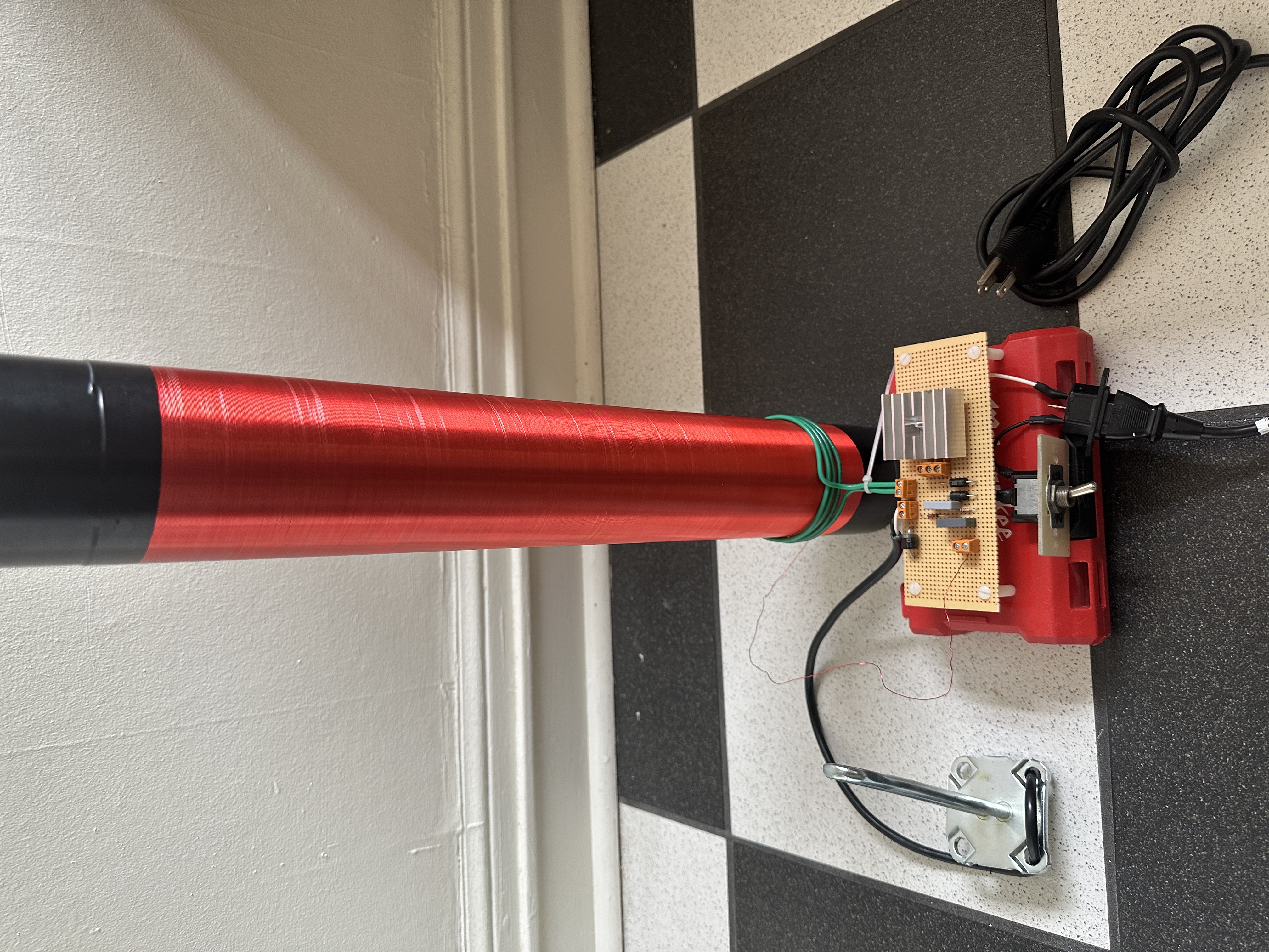
The secondary coil constructed for this circuit has a 3 inch (7.62 cm) outer diameter (OD), with a height of 18.23 inches (46.3 cm) and approximately $1.10\times10^3$ turns (calculated as a ratio of winding length to wire diameter). The primary coil is made of 4.0 turns of 12 American Wire Gauge (AWG) wire with a diameter of 3.06 in (7.76 cm).
Using these values and applying Eq. 4 to find the self-capacitance of the secondary, $$\begin{align} C_{self}\ (pF)= 0.92(7.62) = 7.01\ pF. \end{align}$$ Applying Eq. 5 to calculate the inductance $L_s$ of the secondary coil, with results in $\mu H$, $$\begin{align} L_s (\mu H)&= \frac{1.50^2(1.10\times10^3)^2}{9(1.50)+10(18.23)}\nonumber\ &= 1.40\times10^3\ \mu H = 14.0\ mH. \end{align} $$ Finally, substituting the above results into Eq. 3, $$\begin{align} f_0 = \frac{1}{2\pi\sqrt{(7.01\ pF)(14.0\ mH)}} = 510.\ kHz, \end{align}$$ the theoretical resonance frequency is calculated at 510 kHz.
To confirm the calculated inductance of the secondary coil, a MingHe LC200A inductance meter was connected to the coil, which was held by its ends away from other surfaces during measurement. The inductance of the primary coil was also experimentally measured, as the ratio of its diameter to height was less than 0.8, thus disallowing use of the theoretical calculation. The measured inductance of the secondary was 14.12 mH, and the primary was 4.267 $\mu $H. This agrees well with the theoretical secondary inductance, indicating a strong basis for experimental confirmation of the theoretical resonance frequency.
At resonance, the impedance of an inductor in a series RLC circuit is at its minimum. On this basis, the resonant frequency of the secondary was experimentally tested by creating a voltage divider with a 10 k$\Omega$ resistor (this value was not essential, any large resistor would work), to which one end of the inductor was attached in series, while the other was left floating to form a capacitive coupling to ground.
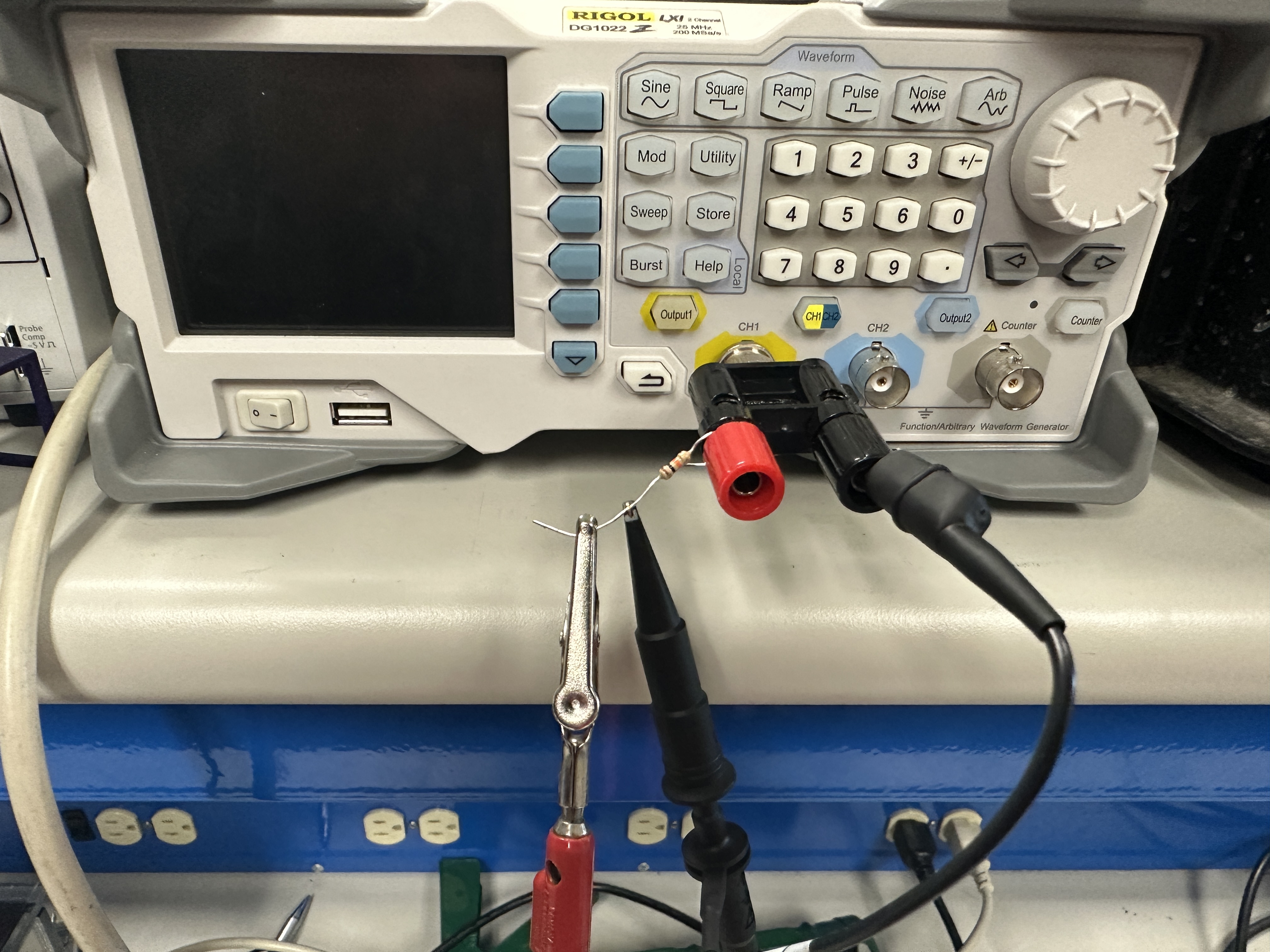
An oscilloscope voltage probe was connected between the bottom of the resistor and the negative terminal on the signal generator, and a 5 V peak-to-peak sine wave was applied to the circuit. Frequency was slowly swept upwards from 1 kHz while the amplitude of the output waveform was monitored on the oscilloscope for a minimum. This point represents the minimum impedance of the coil; its resonance frequency. Fig. 1 shows the signal generator configuration. Using this method, the resonance frequency was experimentally found to lie at 516 kHz.
Using Eq. 2, the induced voltage on the secondary can be calculated $$\begin{align} \varepsilon_s=170\ V \frac{1.10\times10^3}{4.0} = 47\ kV. \end{align}$$
The current limiting ballast chosen for this circuit was a 1500 W water tank heater rated for use on a standard 15 A 120 V residential circuit, with a measured cold resistance of 9.1 $\Omega$. In theory, the instantaneous maximum current that could pass through the circuit, in the case of a dead short beyond the ballast, can be found using Ohm's Law and the cold resistance: $$\begin{align} 170\ V = I(9.1\ \Omega) \ I = 19\ A. \end{align}$$ However, the actual risk of this much current flowing is nonexistent, since resistance for dissipative elements increases with temperature, and temperature increases based on the flow of current. As a result, for a dead short across the circuit, the true maximum current can be calculated using the power equation, $$\begin{align} P=IV, \end{align}$$ bearing in mind that the manufacturer-stated power level is based on 120 V RMS mains voltage, and the peak current will be proportionately higher than the RMS current by a factor of $\sqrt{2}$. Additionally, since the current is half-wave rectified, only half of the power will be available to produce heat, so the true power is closer to 750 W. Then, from Eq. 14, $$\begin{align} I = \frac{750\ W}{120\ V}\sqrt{2} = 8.8 A. \end{align}$$ All components were therefore rated to support at least 10 A of power.
Peak voltage at the MOSFET gate connected to the voltage divider can be considered as two connected cycles: one when the MOSFET is open and current flows through the primary inductor, and one when the MOSFET is closed, and current flows only through the voltage divider. The reactance of the primary coil and the resistance of the ballast will be small compared to the resistance of the voltage divider, however, so the voltage at the top of the divider will roughly follow the mains voltage in both cases. To find the peak voltage at the gate, the equivalent value of both resistors in the branch must be calculated: $$\begin{align} 30.1\ k\Omega + 1.0 k\Omega = 31.1 k\Omega. \end{align}$$ The peak gate voltage can then be determined by considering the proportional voltage drop at the final resistor based on the overall resistance of the circuit, or $$\begin{align} V = 170 V \frac{1.0\ k\Omega}{31.1\ k\Omega} = 5.5 V. \end{align}$$
Circuit Construction and Operation Principle
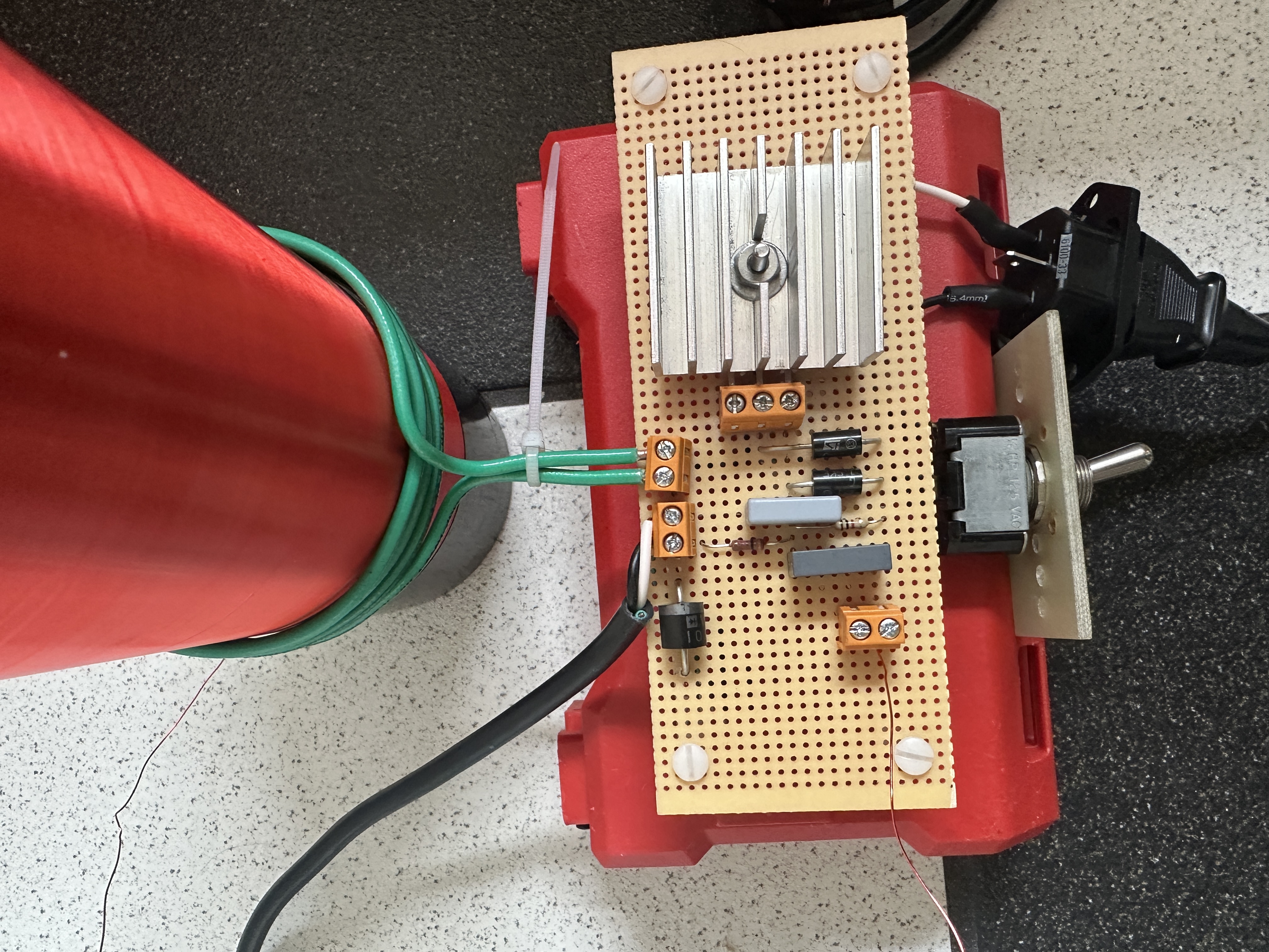
The circuit diagram shown in Fig. 1 was used as a schematic for circuit construction. Incoming 120 V root mean square mains power is half-wave rectified by a 10A10-T diode with a forward current rating of 10 A and reverse voltage breakdown of 1 kV. The current then passes through a 1500 W water heater element serving as a current-limiting resistive ballast. A 100 nF capacitor smooths the half-wave signal, while a voltage divider of 30.1 k$\Omega$ and 1 k$\Omega$ resistors, rated at 1/4 W and 250 V AC, is placed in parallel. The gate of an IRFP460 MOSFET, rated with a drain to source voltage (V$_{DS}$) of 500 V, a continuous discharge current of 20 A, and turn on voltage V$_{GS}$ of 10 V, is connected to the center of the voltage divider. Also connected to this point is a 470 pF isolation capacitor, rated to 500 V AC, which connects to the secondary coil to ensure that mains current does not reach the coil for user safety. Bidirectional transient voltage suppressor (TVS) diodes are placed between the gate and ground, and between the drain and source to clamp voltage spikes that exceed the allowed ratings of the MOSFET.
The coil was wound on a metal lathe with a custom-machined attachment to support the form at the tailstock. The lathe was run at its lowest rotational speed, with the coil of magnet wire supported by a rod and clamped to a heavy stand approximately two meters away to allow a buffer space to correct for kinks and winding anomalies in the coil. Lines were drawn on the form with permanent marker to indicate the 46.3 cm range to be wound. The coil was wound onto an acrylic tube form using 26 AWG insulated magnet wire with a measured diameter of 0.42 mm, including insulation, and was spray-finished with gloss polyurethane to hold the coils in place and provide additional protection.
An unclad phenolic perforated assembly board was used for circuit assembly to prevent arcing between the copper pads present on typical perfboards. Threaded nylon spacers were used in the corners of the board as standoffs, to protect the soldered underside of the board from contacting any conductive surfaces. Screw terminals were used to make replacement of burnt out MOSFETs simpler, as the circuit design was optimized. A large heatsink was specially machined to attach to the back of the MOSFET, and coupled using thermally conductive rubber and machine screws. Finally, a toggle switch rated for 20 A at 120 V and IEC320 C13 female plug adapter were attached for powering the circuit.
Results and Error
For safety reasons, the circuit was operated with two individuals present, one to control the switch on the device an one at the wall to remove the plug if necessary.
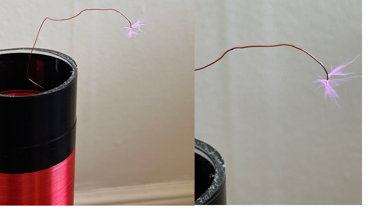
A Kill A Watt current meter was plugged into the wall, and used to measure the current draw of the circuit. The measured value of current draw was 2.48 A when plasma discharge began occurring from the top of the coil.
The circuit was only able to operate for about 30 seconds before failing, and a multimeter with a capacitance and diode measuring function was used to diagnose failed components. The rectifier was tested and determined to be functional, and the values of each capacitor remained in their expected range. The MOSFET was finally removed from the circuit and tested using a practical ad-hoc method, whereby the internal capacitance of the gate was charged using the multimeter, and the gate and source were shorted as the multimeter was monitored for an open circuit. As expected, the MOSFET was demonstrated in this way to be the failure point in the circuit.
Though the circuit did function, one possible reason that it failed after such a short amount of time is that the MOSFET was not fully turned on in the duty cycle. The full turn on voltage for an IRFP460 is stated by the manufacturer as 10 V, but the calculated peak voltage at the gate was only 5.5 V. If the MOSFET was not fully on, or if the ramp up was too gradual, the drain-to-source resistance could have been high enough to cause the power dissipation within the MOSFET to exceed the manufacturer ratings, causing it to dissipate excessive heat and ultimately fail. To determine whether heat did contribute to the failure of the MOSFET, use of an infrared thermometer could provide accurate feedback on the temperature of the components. By measuring the voltage at the gate using a high frequency oscilloscope, and the differential voltage from drain to source, it is also possible to calculate the current through the MOSFET based on manufacturer tables of resistance for various values of V$_GS$. Testing with different voltage divider values may yield more successful results.
In future testing, applying multiple MOSFETs in parallel could also be explored as an option to decrease the power dissipated in each device.
The method used to determine the resonant frequency of the secondary coil may have error associated with it for a number of reasons. The capacitive coupling of the coil to ground completed the circuit, but the value of this capacitance could vary depending on humidity, the ground surface material, and numerous other factors. Measurements of resonance frequency at multiple locations and under different ambient conditions may yield different results to be averaged and considered.
The process used used for testing the transistor was also not exact, and may not work as reliably as some other methods. While the basic functioning of other components in the circuit was also tested after circuit failure, degredation due to voltage spikes and other damaging effects was not, so if the circuit were to fail again in the future, the components responsible could have been cumulatively weakened over many cycles of operation.
Conclusion
A method for building a simple solid state Tesla coil was outlined and the steps for assembling the coil were detailed. The output voltage was calculated to be 47 kV, with resonance experimentally found at 510 kHz. Maximum currents were calculated to ensure that the components used fell within the specifications of the circuit, and that an appropriate ballast was used.
After approximately 30 seconds of continuous operation, the design failed. The failure point of the circuit was determined, and possible reasons for the failure were analyzed. Further testing to determine the root cause of failure is necessary, and may require temperature measurements of the MOSFET, as well as high-frequency voltage monitoring at the gate to determine whether the MOSFET is turning on fully. In future testing and research, the possibility of using multiple MOSFETs in parallel may be explored, so as to decrease the current through each component.